Electrical Probing and Failure Analysis

With our partner Imina Technologies in Switzerland, we offer unique high-resolution probing and manipulation systems which enable researchers to interact and connect to specific areas of their samples under a microscope. The systems we provide are highly modular, ranging from a single probe to 8 independently controlled probes, each mounted to a compact, mobile miBotâ„¢ robot. The sharp probes can be positioned very precisely to make electrical or mechanical contact to the sample in order to make qualitative or quantitative measurements. Different levels of precision are available in the micron or nanometre regime in order to better suit the manipulators to the imaging resolution of the microscope, be that an optical microscope or a Scanning Electron Microscope (SEM)
 

For more information

Electrical Probing and Failure Analysis

With our partner Imina Technologies in Switzerland, we offer unique high-resolution probing and manipulation systems which enable researchers to interact and connect to specific areas of their samples under a microscope. The systems we provide are highly modular, ranging from a single probe to 8 independently controlled probes, each mounted to a compact, mobile miBotâ„¢ robot. The sharp probes can be positioned very precisely to make electrical or mechanical contact to the sample in order to make qualitative or quantitative measurements. Different levels of precision are available in the micron or nanometre regime in order to better suit the manipulators to the imaging resolution of the microscope, be that an optical microscope or a Scanning Electron Microscope (SEM)


Key Features


Applications of the miBot probers include:

Electrical probing

Measure the electrical properties of semiconductor devices on the smallest technology nodes.

Failure analysis

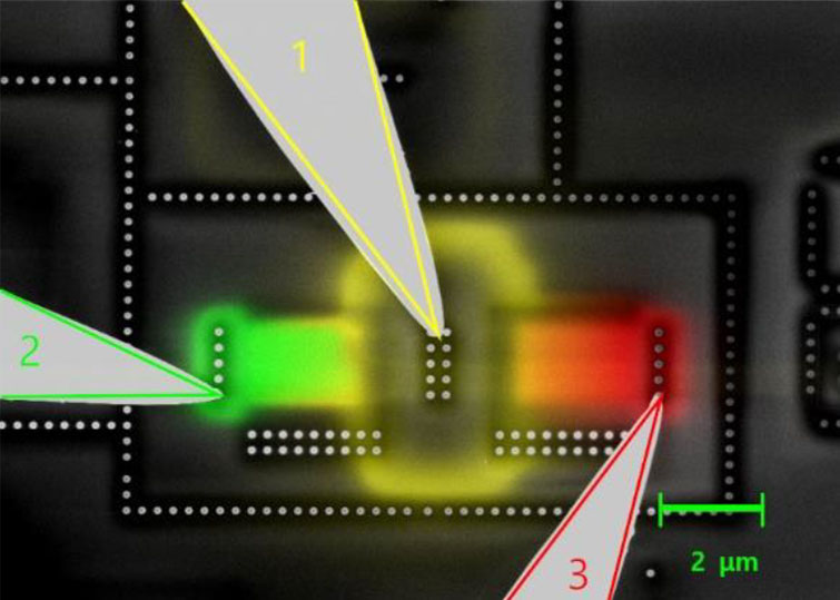
Localise defects at contact levels and metal lines and increase the reliability of semiconductor chips. Complete solutions are available for techniques such Electron Beam Induced Current (EBIC) and Electron Beam Absorbed Current (EBAC). To provide a complete electrical solution, Imina partners exclusively with Point Electronic and the two companies work closely together to provide integrated software for streamlined measurements.

Manipulation

Isolate single particles, perform nano or micro assembly or prepare samples for further investigations.

Custom solutions

We are experienced in integrating our probers on custom stages for different types of equipment where they find unique applications. Special solutions include setups for integration in Atomic Force Microscope (AFM) and Nanoindentation systems from many leading manufacturers.

The MICRO product line has several different platforms that accommodate up to 8 miBotâ„¢ microprobers. Stand-alone MICRO solutions include a microscope and a sample positioning stage. We also offer microprobing platform kits for flexible integration with other microscopy equipment. Each solution enables the user to independently position probes over millimeters with a resolution down to a few tens of nanometers. miBots can also be used to hold optical fibers, sensors, etc.

Up to 8 miBotâ„¢ nanoprobers can be delivered in various configurations and options to adapt to your specific application requirements and microscopy equipment. The compact and light platforms for the robots are compatible with any electron microscope and can either be mounted on the SEM sample positioning stage, or be loaded via the SEM load-lock.

Electrical Probing and Failure Analysis

With our partner Imina Technologies in Switzerland, we offer unique high-resolution probing and manipulation systems which enable researchers to interact and connect to specific areas of their samples under a microscope. The systems we provide are highly modular, ranging from a single probe to 8 independently controlled probes, each mounted to a compact, mobile miBotâ„¢ robot. The sharp probes can be positioned very precisely to make electrical or mechanical contact to the sample in order to make qualitative or quantitative measurements. Different levels of precision are available in the micron or nanometre regime in order to better suit the manipulators to the imaging resolution of the microscope, be that an optical microscope or a Scanning Electron Microscope (SEM)


Key Features


Applications of the miBot probers include:

Electrical probing

Measure the electrical properties of semiconductor devices on the smallest technology nodes.

Failure analysis

Localise defects at contact levels and metal lines and increase the reliability of semiconductor chips. Complete solutions are available for techniques such Electron Beam Induced Current (EBIC) and Electron Beam Absorbed Current (EBAC). To provide a complete electrical solution, Imina partners exclusively with Point Electronic and the two companies work closely together to provide integrated software for streamlined measurements.

Manipulation

Isolate single particles, perform nano or micro assembly or prepare samples for further investigations.

Custom solutions

We are experienced in integrating our probers on custom stages for different types of equipment where they find unique applications. Special solutions include setups for integration in Atomic Force Microscope (AFM) and Nanoindentation systems from many leading manufacturers.

Imina’s Nano robots are the most important components of their probing and manipulation solutions, designed for customers who wish to use them in an SEM environment. They are extremely compact mobile cubes of just over 2x2cm horizontally, and with a low height of just 12.5mm above the stage they are compatible even with short working SEMs. They are fully mobile actuators with the freedom to move at different speeds over the stage on which they sit in X, Y and rotation. Additionally the probe arm is able to move independently in Z. There are two different versions of the Nano robot with different scanning range in the Z axis. The longer travel version facilitates easier approach of the probe to fragile samples and easier switching between different areas of the sample.

Imina’s Micro robots are the most important components of their probing and manipulation solutions, designed for customers who wish to use them in an optical microscope environment, or in an SEM environment where the highest level resolution is not required. They are extremely compact mobile cubes of just over 2x2cm horizontally, and with a low height of just 12.5mm above the stage they are compatible even with short working distance microscope objectives and SEMs. They are fully mobile actuators with the freedom to move at different speeds over the stage on which they sit in X, Y and rotation. Additionally the probe arm is able to move independently in Z.

This probe station is designed for semi-automated electrical characterisation of sub-micron scale components on wafers up to 4’’. The platform drives up to 8 miBot probers and connects their probe tips to third-party electrical source-measurement units. A highly precise X-Y-Z wafer chuck (cooling/heating options available) and a powerful microscope with motorised zoom are part of this fully integrated solution. Automated probing of identical devices across the wafer can be included in this solution.

This compact table-top Probe Station is designed for micro-scale electrical characterisation of semiconductor dies and test devices under 1’’. It drives up to 4 miBot probers and connects their probe tips to third-party electrical source-measurement units. A high-magnification microscope with motorised zoom and a manual X-Y stage for sample positioning are included in this turnkey solution.

Designed to enhance existing microscopy setups and to add electrical characterisation or manipulation capability to virtually any system. Typically this stage is integrated into existing optical microscopes and can accommodate up to 4 miBotâ„¢ micro probers

SEM-Mounted platform for up to 4 miBotâ„¢ nanoprobers including the electrical connections to the robots, electrical feedthrough and customisation for your SEM system. Central mounting point for an SEM sample stub.

SEM-Mounted platform with a wider design to accomodate up to 8 miBotâ„¢ nanoprobers including the electrical connections to the robots, electrical feedthrough and customisation for your SEM system. Central mounting point for an SEM sample stub.

A load-lock-transferrable SEM-Mounted platform for up to 4  miBot™ nanoprobers including the electrical connections to the robots, electrical feedthrough and customisation for your SEM system. Central mounting point for an SEM sample stub.

A larger load-lock-transferrable SEM-Mounted platform for up to 8 miBotâ„¢ nanoprobers including the electrical connections to the robots, electrical feedthrough and customisation for your SEM system. Central mounting point for an SEM sample stub.

The Large Sample Adapter (LSA) fits up to 4 miBots and is mounted on a Nanoprobing Stage (SM100 or SM125). It provides space below for large/tall samples. The LSA is mounted on the Nanoprobing stage with a manual knob and requires no tools for installation/ removal

Our smallest and most flexible stage, designed to accommodate a single miBotâ„¢ micro prober. Designed to enhance existing microscopy setups and to add electrical characterisation or manipulation capability to virtually any system.

Control unit for up to 4 miBotâ„¢ probers. The control unit comes with a control pad and a licence for Imina’s Precisioâ„¢ software Basic Edition

Move the sample independently from the probes in X, Y, Z directions with nm resolution. Reduce probe landing time and accelerate multiple device characterisation.

Vibration-free thermal stage for precise temperature control in the range from -30°C to 150°C. Flexible radiator can be folded to fit the thermal stage into small SEM chambers.

This tool holder enables to easily attach an glass micropipette to the arm of the miBotâ„¢ positioner in order to facilitate precise delivery of liquids into a sample. This can be useful for sample preparation applications or interacting with biological samples especially. The pipette tip can be positioned within a centimeter range cubic workspace with high resolution.

This tool holder enables to easily attach an optical fibre to the arm of the miBotâ„¢ positioner. The fibre tip can thus be positioned within a centimetre range cubic workspace with nanometre resolution. The self-alignment of the fibre on the holder is ensured by a v-groove. A spring loaded clamping mechanism adapts to various fibre optic radius and allows to quickly adjust the fibre length.