Spectroscopy

VSM Instruments offers a variety of spectroscopy solutions to enable surface chemical analysis at a variety of spectral and spatial resolutions and to suit many different budget levels.

Surface sensitive spectroscopic methods, like Auger Electron Spectroscopy (AES), Low Energy Ion Scattering Spectroscopy (LEIS) and especially X-ray or UV excited Photoelectron Spectroscopy (XPS and UPS) have become powerful tools to characterise the surface chemical composition, the chemical state of the surface electrons and the electronic properties of materials surfaces.

Modern related methods can give insight into the surface chemical structure in 2 and 3 dimensions via surface imaging or imaging combined with depth-profiling. Mapping via XPS, or Laser Induced Breakdown spectroscopy, or surface chemical microscopy techniques such as Scanning Auger Microscopy (SAM) can give a complete chemical picture of the surface. The electronic and magnetic structure is also accessible via Angle Resolved or Spin Resolved Photoelectron Spectroscopy (ARPES or Spin-PES).

For several years it has also been possible to perform some of these spectroscopic methods also under environmental or Near Ambient Pressure (NAP) conditions, rather than in Ultrahigh Vacuum (UHV) to allow for operando characterisation of surface chemical reactions or the characterisation of liquids or gases and their interfaces to solids.

For more information

Spectroscopy

VSM Instruments offers a variety of spectroscopy solutions to enable surface chemical analysis at a variety of spectral and spatial resolutions and to suit many different budget levels.

Surface sensitive spectroscopic methods, like Auger Electron Spectroscopy (AES), Low Energy Ion Scattering Spectroscopy (LEIS) and especially X-ray or UV excited Photoelectron Spectroscopy (XPS and UPS) have become powerful tools to characterise the surface chemical composition, the chemical state of the surface electrons and the electronic properties of materials surfaces.

Modern related methods can give insight into the surface chemical structure in 2 and 3 dimensions via surface imaging or imaging combined with depth-profiling. Mapping via XPS, or Laser Induced Breakdown spectroscopy, or surface chemical microscopy techniques such as Scanning Auger Microscopy (SAM) can give a complete chemical picture of the surface. The electronic and magnetic structure is also accessible via Angle Resolved or Spin Resolved Photoelectron Spectroscopy (ARPES or Spin-PES).

For several years it has also been possible to perform some of these spectroscopic methods also under environmental or Near Ambient Pressure (NAP) conditions, rather than in Ultrahigh Vacuum (UHV) to allow for operando characterisation of surface chemical reactions or the characterisation of liquids or gases and their interfaces to solids.

Key Features


  • Wide range of spectroscopic surface analytical techniques from leading suppliers
  • Contact us to discuss your application

While XPS is typically focussed on the chemical structure of a material, UPS (Ultraviolet photoelectron Spectroscopy) and Angular resolved photoemission spectroscopy (ARPES) are focussed on the electronic structure of the material. Compared to XPS, the use of an ultraviolet light source restricts the energy of the photons such that only the valence band electrons of the material are probed.  In UPS and XPS the primary focus is the energy of the emitted electrons, while in ARPES the angular distribution of the emitted electrons is measured in addition to their energy. The emission angle of the electrons is determined by the in-plane momentum of the electron within the surface and can be used to obtain useful information about the electron band structure of the material. The valence band electrons in a material are important to determine the chemical reactivity and electrical properties of the material. With ARPES it is possible to directly determine the band structure of the occupied and unoccupied states.

With our partner, SPECS, we are able to offer ARPES systems with ultimate energy and angle resolution and with highly optimised system properties such as low residual magnetic field, ultralow sample temperature and sample geometry. We also offer a range of high intensity, small spot ultraviolet light sources available as separate components for existing UPS systems.

Auger Electron Spectroscopy utilises a high energy, small spot electron beam to excite surface electrons from the top 3-10nm of the sample. Atoms that are excited by the primary electron beam can relax by the emission of electrons known as Auger electrons. The energy of these emitted electrons is characteristic of the elements present at the surface. The smaller spot size of the electron beams used for Auger analysis mean that the technique can be well suited to imaging applications.

With our partner, SPECS, we offer a small spot size electron source as well as hemispherical analysers that can equally well perform Auger measurements as they can XPS. Auger electron spectroscopy is also integrated into some of our complete systems.

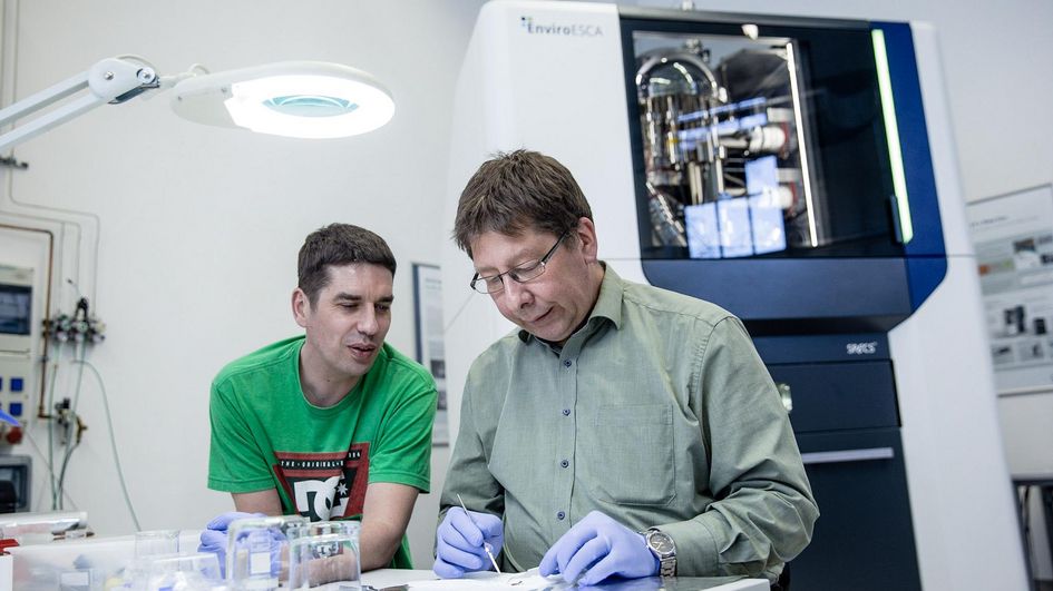
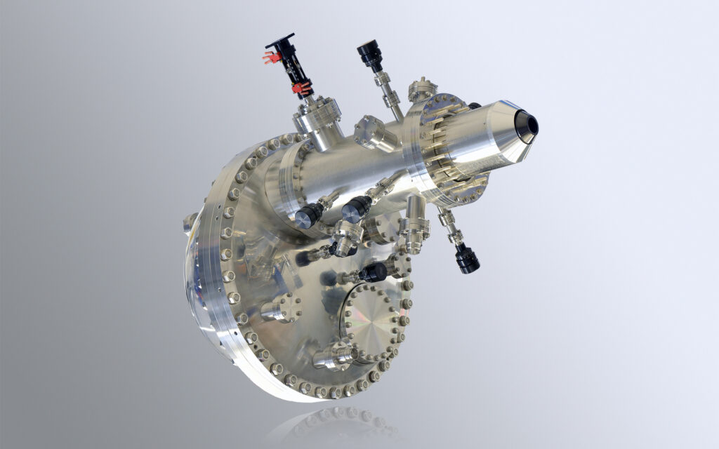
Historically X-Ray Photoelectron Spectroscopy (XPS) was a technique which had to be performed in high or ultra-high vacuum (<~10-7 mbar) due to the limited path length of the electrons emitted from the sample at higher pressures. As a result of advances in the technology commercialised by our partner, SPECS, it is now possible to measure samples at pressures much closer to atmospheric pressure (<100mbar). Analysis at such pressures without pumping the analysis chamber down to HV or UHV conditions first, opens up a much wider range of samples and applications for XPS than were possible in the past. Studies of samples such as liquids, liquid-solid interfaces and samples under a background of different gases become possible. Product development of the X-Ray source technology has also allowed the analysis that would have been performed at a synchrotron in the past to be successfully performed in the customer’s own laboratory. Operating in near-ambient conditions also makes analysis of electrically insulating samples such as plastics or ceramics much easier. Samples which would become electrically charged in conventional UHV XPS are self-neutralised under such conditions. SPECS has become the market leader in this technology and offers a variety of products including a fully automated, high throughput system, the EnviroESCA, as well as systems which offer a flexible approach including UHV analysis and integration of a wide range other UHV techniques.

Conventional X-Ray Photoelectron Spectroscopy (XPS) is a surface-sensitive probe of the sample chemistry with an information depth of approximately 1 – 2.5nm or <10 atomic layers. It uses an X-Ray photon energy of ~1.5keV. In HAXPES higher energy X-Rays in the range of 3-15keV are used which allows a much greater information depth up to ~25nm to be probed. This enables measurements of buried interfaces and bulk properties that would be impossible with conventional XPS.

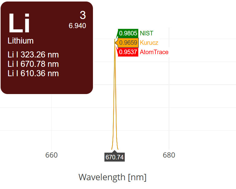
Laser-Induced Breakdown Spectroscopy (LIBS) is an analytical technique used to determine the elemental composition of materials. It employs a focused, high-energy laser pulse to ablate a small amount of material from the surface of a sample, creating a plasma. This plasma contains excited atoms, ions, and electrons from the ablated material.

As the plasma cools, the excited species emit light at characteristic wavelengths, specific to the elements present. A spectrometer collects and analyses this emitted light, producing a spectrum that reveals the material’s elemental composition.

Low Energy Ion Scattering (LEIS) is a special surface analysis technique which is optimised to provide information on the surface composition of only the uppermost layers of the surface. While other techniques such as TOF-SIMS and XPS provide a much greater information depth. Information on the surface layer is especially valuable since the outer surface of the material is of primary importance in determining its physical and chemical interactions.

XPS or X-Ray Photoelectron Spectroscopy is a well-established quantitative surface-sensitive analysis technique. It is sometimes also known as ESCA (electron spectroscopy for chemical analysis). Quantitative Information can be obtained on the surface elemental composition as well as the chemical state of the atoms that are present. In order to obtain XPS spectra, the sample is irradiated with (often monochromatic) X-rays and the characteristic energy of the emitted photoelectrons is measured.

Our product range includes complete turn-XPS systems from our partner, SPECS. These systems can be highly automated and standardised, but can also be customised according to customer requirements.  Given the large number of XPS systems already in the field, there is also a considerable market for upgrade of retrofittable components such as X-ray sources and analysers.

Spectroscopy

VSM Instruments offers a variety of spectroscopy solutions to enable surface chemical analysis at a variety of spectral and spatial resolutions and to suit many different budget levels.

Surface sensitive spectroscopic methods, like Auger Electron Spectroscopy (AES), Low Energy Ion Scattering Spectroscopy (LEIS) and especially X-ray or UV excited Photoelectron Spectroscopy (XPS and UPS) have become powerful tools to characterise the surface chemical composition, the chemical state of the surface electrons and the electronic properties of materials surfaces.

Modern related methods can give insight into the surface chemical structure in 2 and 3 dimensions via surface imaging or imaging combined with depth-profiling. Mapping via XPS, or Laser Induced Breakdown spectroscopy, or surface chemical microscopy techniques such as Scanning Auger Microscopy (SAM) can give a complete chemical picture of the surface. The electronic and magnetic structure is also accessible via Angle Resolved or Spin Resolved Photoelectron Spectroscopy (ARPES or Spin-PES).

For several years it has also been possible to perform some of these spectroscopic methods also under environmental or Near Ambient Pressure (NAP) conditions, rather than in Ultrahigh Vacuum (UHV) to allow for operando characterisation of surface chemical reactions or the characterisation of liquids or gases and their interfaces to solids.

Key Features


  • Wide range of spectroscopic surface analytical techniques from leading suppliers
  • Contact us to discuss your application

EnviroMETROS is a unique metrology platform for the chemical analysis of ultrathin films and 2D materials that allows a detailed characterisation of stoichiometries‚ composition and depth distribution of elements. The system combines XPS with an array of optional techniques such as HAXPES, UPS, IPES, AES, REELS, Raman and Infrared spectroscopies. These techniques can be employed on the same sample spot. It can optionally be configured for NAP XPS, but the base model is a UHV load-locked system. Depending on the system configuration, it can be set up for 80x80mm samples or 8″ or 12″ wafers.


The AtomTrace SciTrace is a modular instrument designed from the ground up for high quality Laser Induced Breakdown Spectroscopy (LIBS) Measurements. The instrument can either be configured as a vacuum-based instrument, or as a simple open “cage” chamber where the sample is measured under ambient conditions. The vacuum body provides protection against laser reflections and potentially toxic ablated materials. All windows are covered with laser filters. The system can easily be configured to house multiple lasers all pointing at the sample target for multiple / double pulsed LIBS in order to enhance the detection limits.

The M-Trace is a truly portable solution for Laser Induced Breakdown Spectroscopy (LIBS). Easily transportable by car for in-the-field analysis, the system is an all in one solution for fast, non-destructive chemical analysis. The system can be powered by batteries and weighs less than 30Kg. It uses a class 1 laser so requires no additional laser safety.

This novel and smart analysis tool overcomes the barriers of standard XPS systems by enabling analyses at pressures far above UHV. EnviroESCA is designed from the ground up for high-throughput analysis and opens up new applications in the fields of medical technology, biotechnology and the life sciences.

It offers the shortest loading-to-measurement time on samples of all types including liquids, tissue, plastics and foils, powders, soil, zeolites, rocks, minerals and ceramics

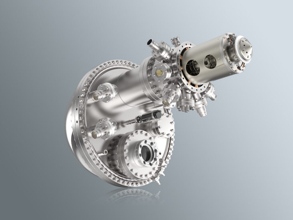
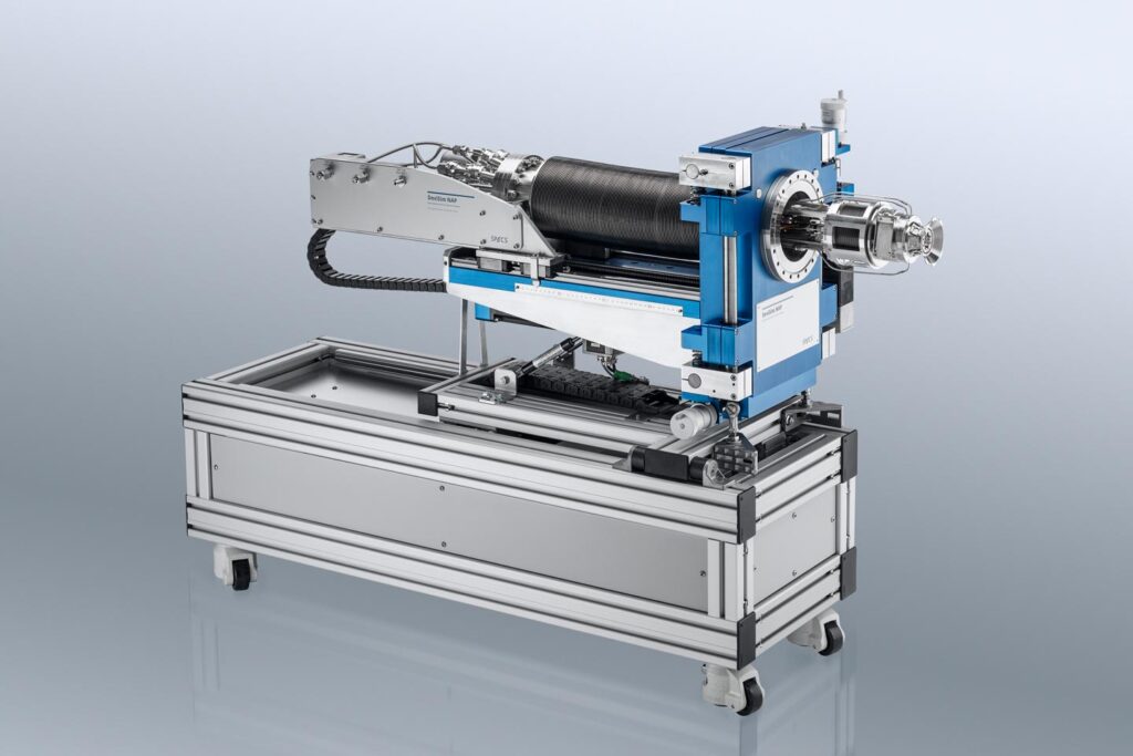
The SPECS ProvenX NAP is available with backfilling configuration or with In-Situ Cell (DeviSIM, like a small compact reactor). It is a performance optimised system for state of the art NAP-XPS as well as NAP-UPS measurements from UHV up to 30 mbar pressure range. It contains a PHOIBOS 150 NAP analyser with unsurpassed transmission and angular acceptance, a high performance small spot monochromatic X-ray source µ-FOCUS 600 NAP, a 4-axes manipulator or DeviSIM with NAP different heating capabilities as well as an optional non-monochromatic UV source UVS 300 NAP.

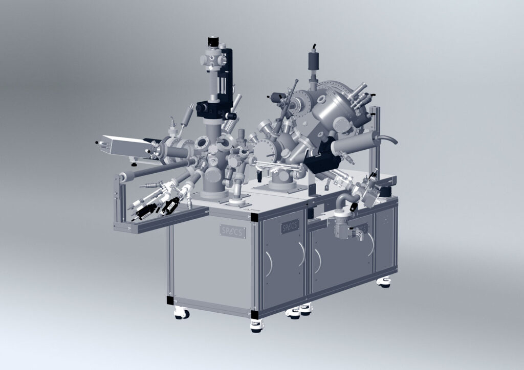
The ProvenX-PS system is a dedicated XPS/UPS system, equipped with PHOIBOS 150 electron analyser with ultra-fast 128 channel delay-line detector with snapshot capability, FOCUS 500 dual anode monochromated X-ray source and optional UVS 10 high-flux UV source. The system comes with a clean UHV sample storage facility and a multi sample fast entry loadlock and can be additionally equipped with a dedicated preparation chamber as well as HPC 20 high pressure cell.

The Qtac is a high sensitivity Low Energy Ion Scattering (LEIS) instrument. It is extremely surface-sensitive, providing quantitative elemental characterisation of the top atomic layer.

This instrument has been developed to include small spot analysis, surface imaging, and both static and dynamic depth profiling.

Its unique surface sensitivity makes the Qtac the perfect tool to study surface processes. The Qtac provides valuable information in many production and research areas on materials such as catalysts, semiconductors, metals, polymers, and fuel cells.

Highest transmission wide angle hemispherical energy analyser with 60° acceptance angle, and AD-CMOS detector for photo electron spectroscopy measurements (XPS and UPS) and angular resolved studies (ARXPS) in the pressure regime from UHV to near ambient pressure (NAP upgradable). With this analyser NAP-HAXPES measurements up to 10 keV can be performed.

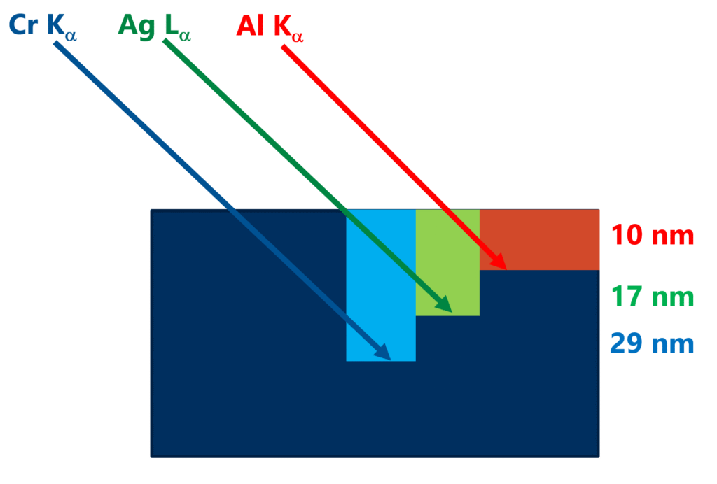
This small spot source is equipped with Al anode in the standard configuration and two upgradable higher energies anodes (Ag, and Cr) for HAXPES capabilities. The µFOCUS 450 monochromator together with the XR-MC micro-focus X-ray source is perfectly suited for small spot, high resolution, and high intensity XPS measurements. The X-ray monochromator operates according to Bragg’s Law of X-ray diffraction. Each wavelength of X-rays (Al Kα, Ag Lα, Cr Kα) is reflected from individually optimized crystals at a specific angle of reflection. For the Al and Ag anodes, quartz crystal are used, which have a 450 mm and 416 mm Rowland circle diameter respectively , whereas for Cr germanium crystals are used with a 676 mm Rowland circle. Due to its overall compactness, the µFOCUS 450 is suitable for mounting on almost any analysis chambers as a bolt-on component. Furthermore, being already equipped with a Si3N4 window, by using the differentially pumped NAP extension, the µFOCUS 450 allows to carry out XPS measurements under gas atmospheres of up to 50 mbar.

The µFOCUS 500/600 monchromator is equipped with microfocus high performance X-ray source XR 50 MF which is specially designed for the use with the monochromator. This small spot source is equipped with Al anode. The small spot monochromator µFOCUS 500/600 operates according to Bragg´s Law of X-ray diffraction. A single wavelength of X-rays is reflected from a quartz single crystal mirror at a specific angle of reflection. A moveable aluminised polymer window (shutter) is provided on the monochromator housing for differential pumping or to shield the crystal assembly during sputtering

The XR 50 is a high intensity twin anode X-ray source optimised for XPS experiments. The anode is made of silver to avoid any CuLα breakthrough. Due to the use of dual anodes it is possible to switch between two different incident energies without the need to vent the system. Dual anodes with different material coatings are available on request including Al, Mg, Ag, Cr, Zr. The electron optical design of the anode, filament and source housing guarantees maximum X-ray intensity and very low crosstalk between the anode faces.

The FG 22/35 is a compact, easy to handle, reliable flood gun for charge neutralisation of positively-charged insulators or semiconductors. It allows operation in the energy range of 0 – 500 eV for charge compensation in typical XPS/AES and SIMS experiments, respectively.

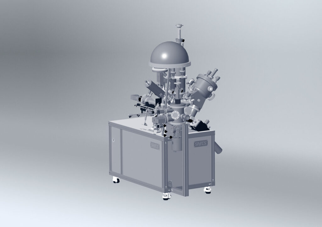
The ProvenX-ARPES system is a dedicated small spot ARPES analysis tool, supporting the new ASTRAIOS 190 electron analyser with single spot shifting lens, parallel single event detectors and optional 3D spin detection, as well as the UVS µFOCAL small spot UV source with optional monochromator. The sample handling is done by the SPECS Ganymed low temperature manipulator series. The system comes with a dedicated preparation chamber, a clean UHV sample storage facility and a multi sample fast entry loadlock.

System control is done by the SpecsLab Prodigy software suite with integrated remote control packages, automated sample handling and a computer based vacuum control system.

The system can be equipped with an optional small spot x-ray source for material characterization, electron sources and charge neutralization sources. Additional software and preparation tools are available.

The ProvenX-MM system is a specialized system base for momentum microscopy solutions, supporting the KREIOS 150 Series, parallel single event detectors and optional spin detection, as well as the UVS µFOCAL small spot UV source with optional monochromator. The sample handling is done by the SPECS HESTIA low temperature microscopy stage. The system comes with a dedicated preparation chamber, a clean UHV sample storage facility and a multi sample fast entry loadlock.

System control is done by the SpecsLab Prodigy software suite with integrated remote control packages, automated sample handling and a computer based vacuum control system.

The system can be equipped with an optional small spot x-ray source for material characterisation. Additional software and preparation tools are available.

The ASTRAIOS 190 is a revolutionary ARPES analyser for 2D momentum mapping. It is based on a direct k-mapping single spot shifting lens with a virtual entrance slit for ultimate k- and energy resolved measurements.


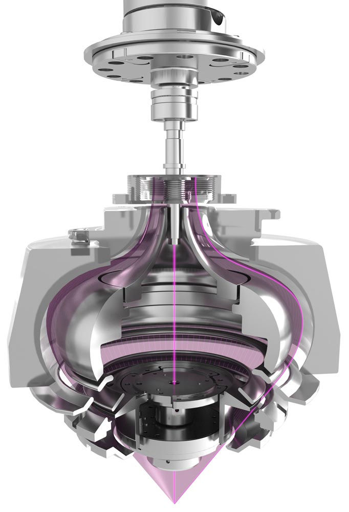
The KREIOS 150 S is a new generation of electron spectrometers for high performance ARPES and PEEM. The unique lens system combines an immersion lens for PEEM operation with a hemispherical energy analyser scanning system for unrivaled ARPES measurements. Its lens system acquires the full half sphere of the electron emission for ultimate angular acceptance of 180°.

The KREIOS 150 S displays energy vs k-vector or energy vs spatial information directly on the detector. With the scanning lens it is possible to measure a full 3D dataset for ARPES or energy filtered PEEM. The lens system features apertures to refine the k-space into high contrast and dark field PEEM, as well as field apertures to select a spatial region for µ-ARPES down to 2 µm field of view. The kinetic energy up to 1500 eV allows XPS and XPEEM measurements. With the new CMOS detector, the KREIOS 150 S is the most performing ARPES analyser available.

The small spot monochromator µ-FOCUS 500/600 NAP is developed for XPS measurements in near ambient pressure regime. The X-ray monochromator operates according to Bragg’s Law of X-ray diffraction. A single wavelength of X-rays is reflected from a quartz single crystal mirror at a specific angle of reflection. The mirror has a 500 mm Rowland circle diameter for µ-FOCUS 500  NAP and 600 mm for µ-FOCUS 600 NAP, respectively. Due to its overall compactness, the µ-FOCUS 500/600 NAP is suitable for mounting on almost any analysis chambers as a bolt-on component. By using the differentially pumped NAP extension with Si3N4 window, XPS measurements under gas atmospheres of up to 30 mbar can be carried out.

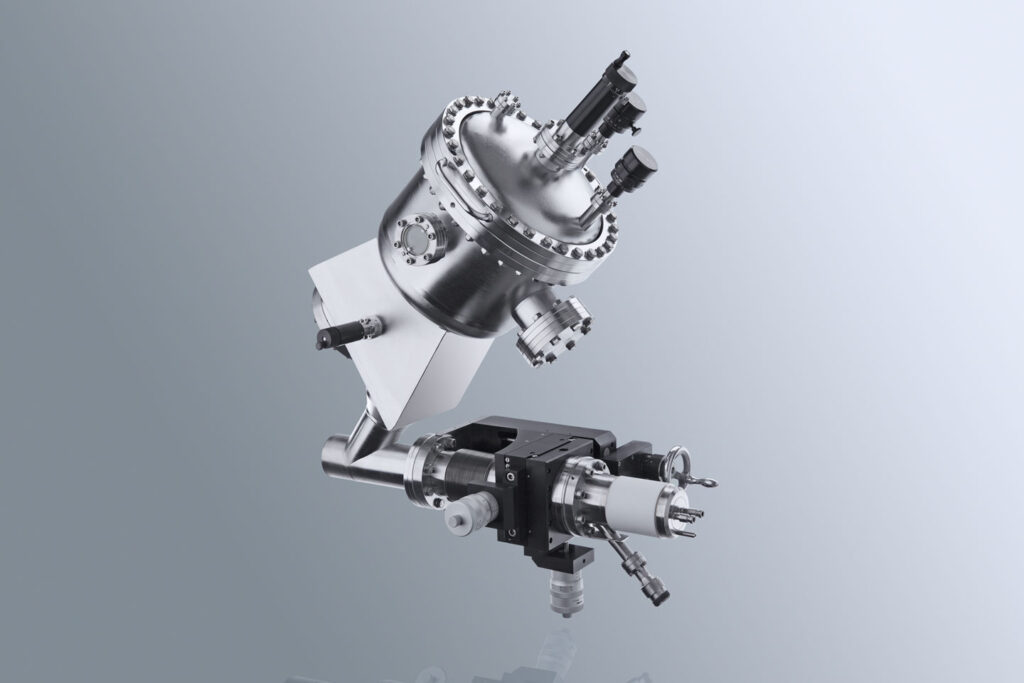
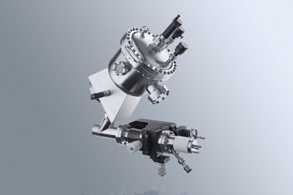
DeviSim NAP is a reactor cell of 400 ml volume at near ambient pressure conditions that can directly be coupled to the PHOIBOS 150 NAP. It is built on a manipulator which is docked into the UHV analysis chamber with PHOIBOS 150 NAP analyser. It designed for a fast sample transfer. The cell includes a gas inlet system suitable for a wide range of gases. The sample heating mechanism allows for heating up to 600 °C at 20 mbar of N2 pressure and cooling with liquid Nitrogen down to at least 200 K and a gas handling system.

This source can be used for almost any application which requires an focused electron beam. Among the popular applications are Auger Electron Spectroscopy (AES), scanning imaging applications (SAM/SEM), electron energy loss spectroscopy (EELS), or electron pulse applications such as desorption (ESD) experiments. Due to the high transmission of its Einzel-lens, the EQ 22/35 is an electron source which gives high electron beam currents over a wide energy range.

The KREIOS 150 MM is a new generation of electron spectrometers for high performance ARPES and PEEM. The unique lens systems combines and immersion lens for PEEM operation with a hemispherical energy analyser scanning system for unrivaled ARPES measurements. Its lens system acquired the fill half sphere of the electron emission for ultimate angular acceptance of 180°.

The KREIOS 150 MM comes with a special lens system for momentum microscopy, showing a constant energy map or a real space map on the detector. Integrated deflectors allow changing the microscopy spot without moving the sample. The lens system features apertures to refine the k-space into high contrast and dark field PEEM, as well as field apertures to select a spatial region for µ-ARPES down to 2 µm field of view. The kinetic energy up to 1500 eV allows XPS and XPEEM measurements. With the new CMOS detector the KREIOS 150 is the most performing ARPES analyser available. Due to the design of the KREIOS lens system and hemisphere, no artificial aberration correction is needed. Instead a second hemisphere can be upgraded to enhance the energy resolution or the electron transmission.

The METIS 1000 is the next generation TOF spectrometer for ARPES and momentum microscopy. If a pulsed light source is available, the METIS 1000 is the intrument of choice. It allows aquisition of two in plane k-vectors against the kinetic electron energy in one shot. The lens system is optimised for high momentum resolution and acquired electrons from the complete half space above the sample, yielding ultimate acceptance angles. The lens design directly shows the k-space on the detector, hence, no conversion from angular space into real space is needed. Integrated deflectors in the microscopy lens allow to move the area of interest without moving the sample and integrated apertures can be used for µ-ARPES or contracst enhancement in PEEM. The native repetition rate of the detector is 5-8 MHz. With a special frequency splitter is is possible to boost the acceptable repetition rate up to 100 MHz.

The µSIRIUS is a new generation of duo-plasmatron based discharge light sources. Its body fully manufactured by additive manufacturing increases the stability and performance compared to the existing UV light sources. The imprinted water cooling reduces the dimensions of the source and allows us to improve the anode geometry. The photon flux density can be increased by an order of magnitude compared to the existing solutions. A new type of filament comes with a significantly increased life time of > 5000 hours.

The µFOCAL capillary is a true focusing capillary. Due to the duo-plasmatron principle, the UV source generates a tiny emission spot, which can be focused on the surface without any artificial apertures. The new capillary design reduces the spot size down to 100 µm with no loss in the photon flux. Hence the flux density on the sample surface can be increased by one order of magnitude.

The TMM 304 is a high flux VUV monochromator optimised for use with the µSIRIUS UV source. It features exchangeable gratings for various emission lines such as He I, He II or Xe. The design of the VUV monochromator produces light with a high intrinsic degree of linear polarized light. A rotatable frame allows a change from s to p polarization without breaking the vacuum. An optional polariser cassette is available to increase the degree of polarisation. The efficient pumping system results in extremely low operational pressures in the analysis system

The SPECS UVS 10/35 is an easy to use and robust UV source. It provides an excellent He I to He II ratio and can be operated with many different gases. The source is designed for longest operation time with extreme stability and easy ignition.

The UV source fits almost any vacuum chamber on a free DN40CF flange, while the sample to flange distance is not critical. An optional polariser is available to polarise the normally unpolarised light.

For many years, the Phoibos-series analysers have formed the cornerstone of the SPECS analyser product range and as such are well proven in the field. Depending on configuration, the Phoibos series can be adapted for XPS, UPS, ARPES, HAXPES, NAP XPS or ISS. It comes in three possible hemisphere sizes: 100, 150 and 225mm and a range of 1D and 2D detectors including 1D and 2D delayline, 2D-CCD and AD-CMOS. Acceptance angles of +/-15º are standard.

Low Energy Electron Diffraction (LEED) is one of the most powerful methods to determine surface structures. Analysis of LEED patterns and intensities provides the size and shape of the surface unit cell, the degree of order and detailed atomic structure with a precision of the order of picometers. Our LEED optics also enable Auger Electron Spectroscopy (AES) when equipped with the appropriate (optional) control unit. AES is a technique to provide chemical analysis of the surface. Our LEED optics are available in two flange sizes, DN100CF and DN150CF. We recommend the largest possible flange size if the chamber allows it, as larger screen sizes much are easier to work with and the cost saving for the smaller optics is minimal.